Detecting faults by looking into what is hidden
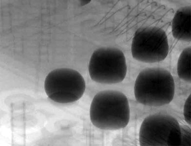
AOI systems inspect the visible quality features of an assembly. But they have a limit: what is hidden from the human eye cannot be inspected optically even by an AOI. Solder joints of components with surface-mounted connections such as BGAs, CSP, Flip-Chip or QFN are often concealed. In some cases, almost every third solder joint is hidden. But the reliability of electronic assemblies is largely dependent on the quality of these solder joints. X-ray inspection makes it possible to look inside the assembly and significantly minimises failures caused by bad solder joints.
Technology
An X-ray source is placed opposite an X-ray image detector and generates X-rays. These are electromagnetic waves similar to light. However, with a much shorter wavelength, they are able to penetrate matter. When an object is penetrated, some of the X-rays are absorbed; the denser the area of the object that is penetrated, the more is absorbed. The detector captures the radiation and displays it in different shades of grey, depending on the intensity. Denser or thicker materials and areas usually appear darker in the digital X-ray image, for example iron or lead. Thinner and less dense areas appear lighter, for example materials such as plastic, paper or air. This creates the familiar X-ray image, which can then be displayed, digitally processed and evaluated.
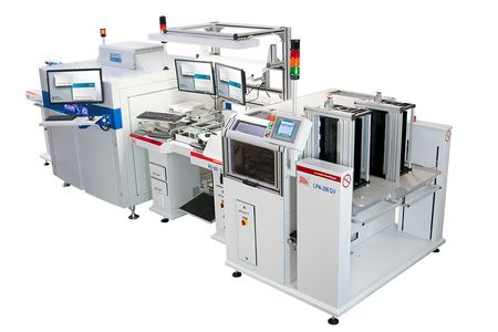
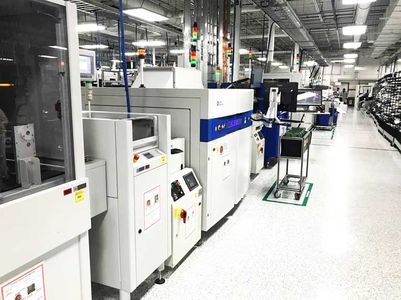
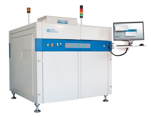
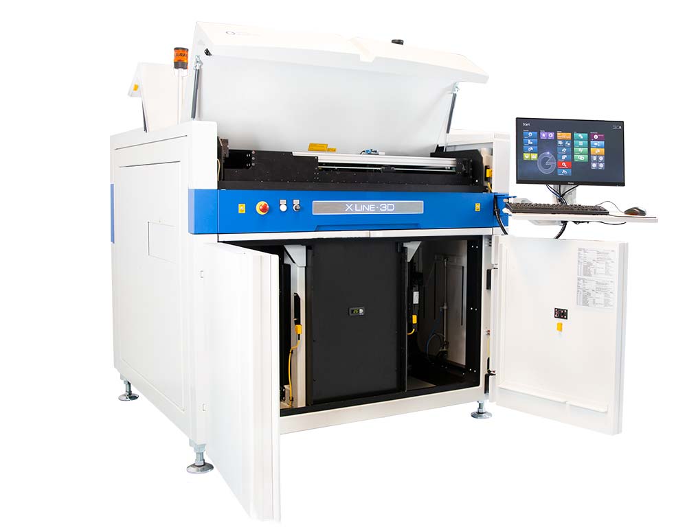
In the automated X-ray inspection of electronic assemblies or components, the UUT is transilluminated by a cone-shaped X-ray beam in a radiation-tight housing. The magnified X-ray image is recorded on a detector underneath. X-ray inspection systems can be used as part of production lines (inline) or as a separately installed inspection island (offline). In both cases, the test object is fed in via belt modules and transported further after inspection. The duration of the fully automatic X-ray process is decisive for the cycle time in the production line. The inline procedure is often used for large-volume production. For prototype analyses, for small quantities or when limited to random samples, X-ray inspection systems are also used as manual systems. In this case, the machine is loaded and unloaded manually, detached from the production line.
Manual and automatic X-ray inspection
Manual X-ray systems, so-called MXIs (Manual X-ray Inspection), are different from the offline X-ray systems mentioned above. They do not offer the possibility of integration into a production line and they are only used to randomly inspect hidden solder joints. They offer a comparatively inexpensive entry into the world of X-ray and can be used for production start-ups and the analysis of prototypes. MXI systems are capable of producing high-resolution X-ray images with a high degree of detail. Similar to a microscope, the user manually inserts an assembly into the system and can generate the "ideal X-ray image" via the free movement of the X-ray image chain and the UUT. The disadvantages of these systems are the manual loading and analysis. A one hundred percent inspection of all manufactured assemblies is usually not possible for reasons of cycle time. Also, an always identical evaluation of the images is not given due to the human factor. Depending on the operator's experience and level of knowledge, the same image can be interpreted differently. In addition, automated logging and archiving of the results and measured values is usually not possible. This is where automated X-ray systems, so-called AXI (Automated X-ray Inspection), come into their own. With a slightly lower resolution and lower level of detail in the X-ray images, AXI systems enable fully automatic loading, inspection, evaluation and result logging of the assemblies. Depending on the requirements, two basic inspection strategies are usually used. On the one hand, there is a need for full-surface X-ray inspection of all components and solder joints, both hidden and visible solder joints, for example on SMD components such as SO-ICs. In other cases, only selected, hidden solder joints need to be inspected with X-ray, as an AOI system, for example, inspects the remaining solder joints. Similar to an AOI system, AXI systems work with a previously parameterised inspection programme to inspect the respective solder joints with image processing algorithms.
Typical AXI applications
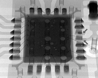
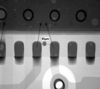
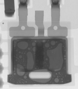
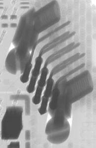
The main task of an X-ray system is the detection of solder defects in both hidden and visible solder joints. In this context, open, lean, greasy and non-soldered solder joints are just as much a part of everyday inspection as voids, vagabond solder balls and short circuits. Modern X-ray systems have a variety of inspection functions to detect these defects. Similar to an AOI system, an inspection programme is created and parameterised on the basis of CAD data. As an example, a BGA inspection includes checking of misalignments, solder bridges, solder joint diameters, head-in-pillow connections and voids. The same applies to components such as QFN (Quad Flat No Leads Package) DFN (Dual Flat No Lead), QFP (Quad Flat Package) and LGA (Land Grid Array). For THT solder joints, the tin penetration can be checked by X-ray inspection, and the rear solder miniscus can be assessed on gullwing pins that are difficult to see. In large solder joints such as DPAK/TO-252 packages, but also in BGA solder joints, the detection of air inclusions (voids) is a particular task.
2D, 2.5D, 3D X-ray technologies
The vertical radiography of a UUT is known as 2D X-ray. Modern electronic assemblies, however, are often characterised by double-sided assembly of the printed circuit board. In the X-ray image, their mutual overlapping as well as the overlapping with vias, bonding wires and conductor tracks can make inspection difficult or even impossible. If an oblique view is taken through the PCB, this is called 2.5D X-ray or oblique projection. The oblique view helps, for example, to assess the tin penetration at THT solder joints or to check the connection of BGA balls. Even with 2.5D technology, there are limitations with PCBs assembled on both sides. Most reliable quality statements, however, can be made with 3D technology. This enables digital micrographs to be displayed. Similar to the medical CT procedure, a 3D reconstruction can be carried out. For example, horizontal and vertical sections through the assembly and its solder joints are possible. 3D X-ray images are always synthetically generated images and are created from a large number of oblique 2.5D images. In AXI systems with digital area detectors ("flat-panel detectors"), 8-16 such oblique images are usually used for 3D image calculation in inline mode. For this reason, 3D AXI systems are always slower than conventional 2D/2.5D devices that only work with one image acquisition. With assemblies assembled on both sides, 3D image acquisition is the only reliable means of obtaining a high degree of optical inspection coverage. With this technology, the solder joints on the top side of the assembly can be separated from the solder joints on the bottom side of the assembly and inspected and evaluated independently of each other.

Detectors and stop-and-go vs. scanning image acquisition
Analogue radiographic films were originally used as detectors. These were replaced by analogue X-ray image intensifiers with CCD cameras, also for use in electronics inspection. Today, it is common to use digital detectors, which have high contrast resolution, dynamic range and low noise. A distinction is made between two types of detectors - CMOS flat-panel detectors and scanning TDI line detectors. Flat-panel detectors are usually used when only individual components of the PCB need to be inspected in 2D, 2.5D or 3D. Flat-panel detectors have a disadvantage when it comes to 3D image acquisition: The oblique radiation images (so-called projections) required for 3D image reconstruction must be acquired using a stop-and-go procedure. The acquisition of an oblique projection always requires an axis movement. The movement time for accelerating and decelerating is significantly longer compared to the exposure time. As a result, the cycle time for inspecting a large number of components in 3D increases rapidly. For a standard 3D image field with eight projections, approx. 3-5s are required. Depending on the placement situation, however, a higher number of oblique projections must often be selected. Often, up to 32 projections are necessary in inline operation to obtain a good inspection depth.
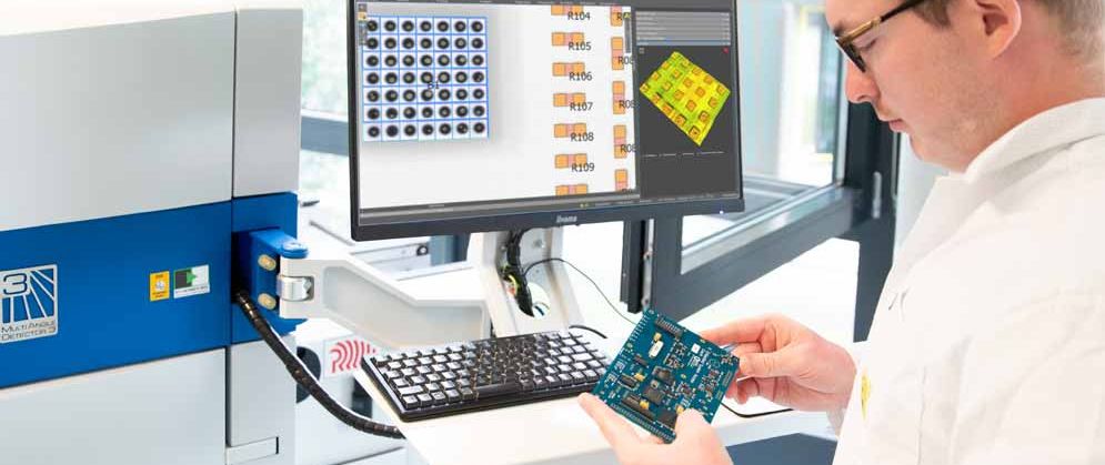
If many components have to be inspected in 3D and with a short cycle time, scanning X-ray imaging with digital line detectors is suitable. For this purpose, GÖPEL electronic has developed its own X-ray detector based on several bidirectional scanning TDI line detectors. The MultiAngle Detector Version 3 offers a fast, parallel X-ray image acquisition of 2D and 2.5D images. The 2.5D images are acquired simultaneously from different directions. The number of 2.5D images used to calculate the 3D image can be freely selected in the software. With scanning image acquisition, the many stop-an-go axis movement times are eliminated. Thus, significantly shorter image acquisition times can be realised. This is particularly interesting when a multiple use with many components is to be inspected in 3D. Another advantage is the larger field of view (FOV).
Radiation exposure for components and operators
X-ray facilities in electronics manufacturing must meet the requirements for full-protection equipment according to the X-ray Ordinance. For this purpose, the X-ray chambers of the facilities are enclosed in lead-lined radiation protection booths. In addition, independent safety circuits ensure that the current flow (and thus the radiation inside) is immediately interrupted when the door is opened. After installation, the facilities are subject to approval and may only be operated by instructed, regularly instructed and trained personnel.
Electronic parts and components are usually not exposed to any danger, as the radiation dose is usually only about one thousandth of the value at which damage would be observed. The systems can additionally control the radiation dose themselves. The AXI systems of GÖPEL electronic reduce the radiation dose for components by several measures. On the one hand, the low-energy radiation components that do not directly contribute to imaging are reduced via suitable filters before the X-ray source. Secondly, the X-ray radiation is interrupted directly after the image acquisition to avoid unnecessary irradiation. If the system is configured with the line detector, the dwell time of the UUT in the beam path is minimised by the fast, scanning image acquisition process with very short exposure times. This further reduces the radiation dose to the components.
 联系我们
联系我们

