Improved inspection of solder pastes, sinter pastes and DCB substrates
New funktions for the SPI Line · 3D
GOEPEL electronic has upgraded the inline inspection system SPI Line · 3D. In addition to 3D solder paste inspection, the SPI Line · 3D now has new features for testing sinter pastes and Direct Copper Bonded (DCB) substrates.
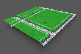
Due to the high precision of the system in conjunction with the new functions, process errors in sinter paste printing can now also be detected. Even the smallest defect structures such as voids and particles with heights below 20 µm can be detected with reproducible results. In addition, the system is now able to inspect DCB substrates. For example, air pockets (voids) on DCB structures can be reliably measured from a height of 10 µm. This makes the SPI Line · 3D the only SPI system currently available on the market that can be used for both traditional solder paste inspection with typical solder paste heights of 80 µm to 150 µm and for the newer applications of sinter paste and DCB testing with significantly lower structural heights.
The system software PILOT SPI provides the user with simple and intuitive test program creation. The operation is possible via touchscreen. Complete test programs can be created in less than 10 minutes.
The PILOT Connect software module connects the system with other inspection systems. This common interface for SPI, AOI and AXI centrally captures and manages all inspection data as well as the machine and operating data of the connected systems. It also allows bidirectional communication to higher level MES and traceability systems.
Furthermore, all inspection information can be merged on a central verification and repair station, combining data to create the safest and most dependable fault assessment environment available along with completely new possibilities for optimizing the production process.
 Contact

