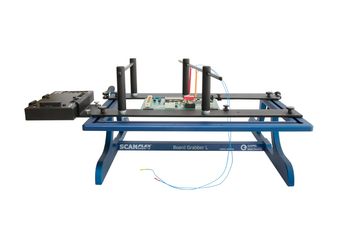
![[Translate to Englisch:] Prototypentest und Debugging mit SCANFLEX Board Grabber [Translate to Englisch:] Prototypentest und Debugging](/fileadmin/_processed_/0/0/csm_board-grabber-tap-transceiver_ce42681ea3.jpg)
The Embedded JTAG Solutions and JTAG/Boundary Scan are not only an effective test procedure for the production of printed circuit boards. It offers many advantages, especially in the development, which enable you as a developer of Printed Circuit Board Assemblies (PCBAs) to find new approaches to solutions and achieve high quality.
This makes it possible to perform a comprehensive test in series quality from the very first prototype. The in-system programming and testing run via the same JTAG interface. And you don't even need a finished firmware. All you need in terms of hardware is a controller for access, e.g. SCANFLEX II CUBE.
The use of Embedded JTAG Solutions based on IEEE 1149.1 has some advantages already in the development phase:
The DFT-Guide (Design-for-Testability) explains what you as a developer should look out for when using Embedded JTAG Solutions.
First of all, you should know which components of which type are on the circuit board and how each pin of the components are connected to each other. The component types must then be assigned to corresponding models. For each Boundary Scan capable component there is a model which describes its Boundary Scan structure - the so-called BSDL (Boundary Scan Description Language) model. Depending on the provider, there are also different models to describe the non-boundary-scan capable devices, such as RAM devices or driver ICs.
The models are supplied by the test system, and the CAD data required is limited to a network and component list. These can be obtained from the schematic, which is usually available at a very early development stage of an assembly. The advantage is that you can easily resolve problems that may occur during test generation. You can also quickly and easily change a design that is unsuitable for test depth. But that's not all!
The generated tests are already usable for the first prototype. From now on, this prototype can be tested with exactly the same quality as the pilot series and ultimately the series product; same test depth, same pin-exact error statement. Since the test bus required for JTAG/Boundary Scan has already been designed to be adaptable on the DUT (e.g. via a connector), the FPGAs or CPLDs can also be loaded via this interface, or the bootloader can be stored in the program flash, thus completing programming. The resulting savings are obvious.
Contact us!

Free Time finished
Please register now to view the whole webinar.
Not a member yet? click here to register. Contact